I have always wanted to build a fairly capable LCR meter that could cope with real world use in my own personal lab. This would mean reasonably good accuracy across a wide range of L, C and R. Fortunately, I got the time to do just that this year in the 3rd year Instrumentation module at my University. Although this justified spending time on such a project, I was motivated to do a good job so the end result would be usable as an actual piece of test equipment.
The approach I took was a mixed signal one where a capable analog front end would be paired up with a beefy DSP processor to compute the Impedance. Most importantly, in this scheme, the DSP is responsible for discriminating the phase between the sampled voltage and current waveforms; this approach is preferred because it leads to good accuracy and calibration stability.
The specifications and features were basically designed to mimic a commercial LCR meter. The test frequencies can be chosen from 1, 10 and 100 KHz and are all digitally synthesised. The software supports displaying L, C, R, Z and also an auto mode that classifies the DUT based on its impedance phase. The impedance measurement range with simple calibration has currently been tested from 0.1 Ohm to 10 MOhm with very good accuracy; this range is achieved by a highly reconfigurable analog signal path that allows about 100 voltage and current ranges, most of which are not used to allow easier calibration.
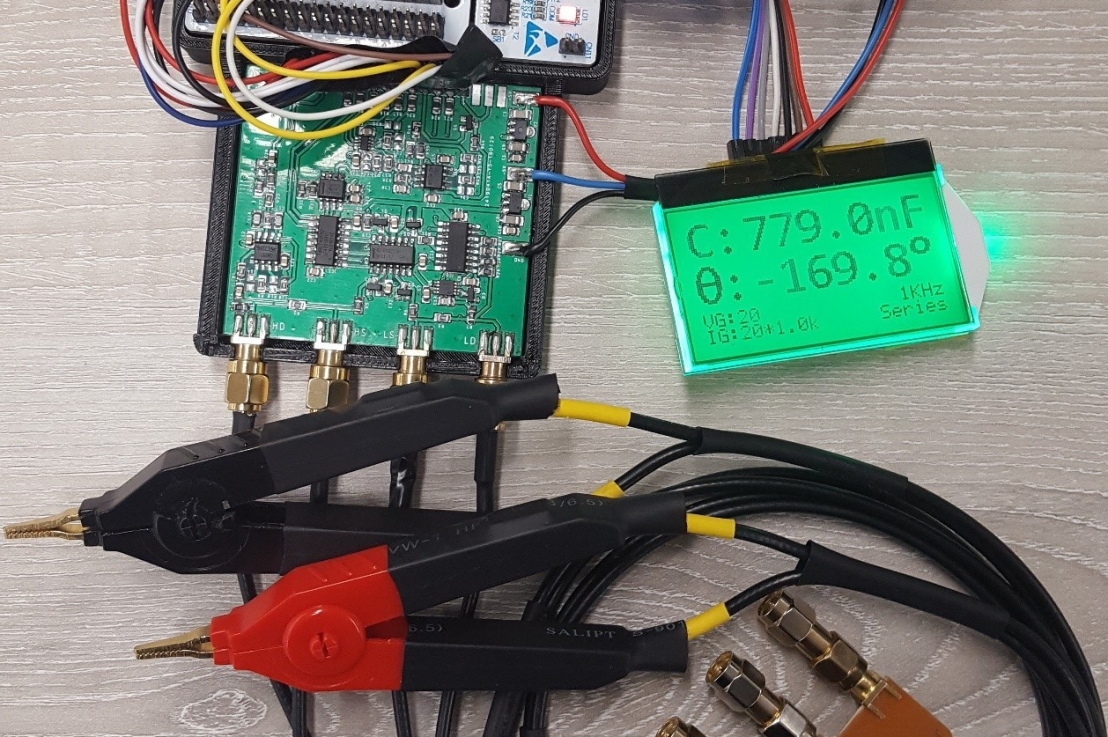
The LCD is a jelly bean 128×64 type and has been divided into a primary display consisting of the measured quantity and a secondary display showing the current measuring range and the impedance representation currently being displayed. The overall cost came to about £55.
Measurement Theory:
Passive Shunt:
The first method is the traditional and broadband technique commonly referred to as the “I-V method”. In this a resistive current shunt is placed in series with the DUT and the voltage across the shunt and the DUT are read off, allowing a calculation of Z.
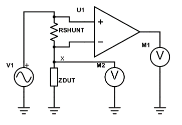
However, this method has severe practical limitations described briefly below.
Limited I-V gain which is coupled to burden voltage: To keep the burden voltage of the shunt small, the shunt itself is typically, a few mOhms. As a result, I-V gain i.e. the differential voltage across the shunt is very small and on top of a much larger common mode signal. This places very strict performance requirements on the difference amplifier U1 and any subsequent gain stages. The only way to practically increase this signal is to increase the value of RSHUNT, which in turn increases the burden voltage. The source V1 then needs to be increased to keep VZDUT, often a strictly specified test parameter, constant
Difficult to employ solid state range switching: One way to overcome the above problem and to accommodate a wider measurement range is to switch in different shunts for different ranges. However, solid-state CMOS switches can have resistances in the range of 20-150ohms and as they would be placed in series with the shunt, would significantly increase the burden voltage requirement of the setup. The relay would also take up substantial board area and have more complicated drive circuitry.
Auto-balance Half Bridge:
A much more practical and heavily employed circuit is the so called auto-balancing bridge(ABB), where the shunt is replaced by a transimpedance I-to-V amplifier. The amplifier can be viewed as performing the role of an “active shunt”, where the burden voltage mimics that of a very small shunt resistor but the I-V gain is that of a much larger resistor! However, as this circuit employs feedback, stability is now an important consideration.
As is assumed to be a virtual ground, the measurement circuit is greatly simplified and the impedance can in theory be measured by simply making two single ended measurements of voltage and current and and then using ![]() .
.
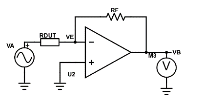
This type of single-ended measurement based circuit is used heavily in lower-end test equipment up to 10KHz with modest accuracy. I opted for the above circuit, albeit with a modification that makes differential measurements across RDUT and RF for utmost accuracy.
Block diagram
After some deliberation I opted for the following arrangement:
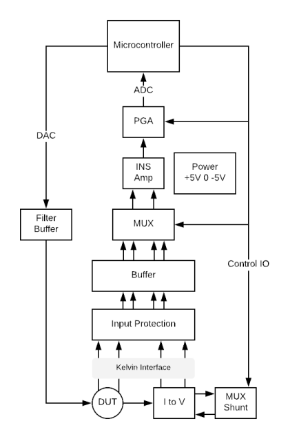
The circuit begins by a 4-wire Kelvin interface (on SMA connectors) to the DUT which has extensive input protection in the form of series resistors and bidirectional low leakage diode clamps. The diode clamps ensure node voltages of the Opamp inputs do not exceed the supply lines. The current is sensed using a TIA which uses a 4-to-1 analog MUX in the feedback loop to select 1 of 4 different precision shunt resistors for the various ranges. The TIA is chosen to have a relatively large GBP (20MHz) to minimise phase shifts and has very low input bias current to minimise errors. However, this is somewhat defeated because we need to severely restrict the bandwidth of this amplifier for stability reasons.
The differential voltage and current lines are first buffered using a quad Opamp and then feed into two, 2-to-1 analog MUX, which connects one of the two selected quantities (voltage or current) to a precision instrumentation amplifier. This keeps the majority of the signal chain identical for both measured quantities, minimising error in impedance calculations. The output of the instrumentation amplifier then connects to a digitally programmable gain amplifier. The output of the PGA is first scaled, then enters an anti-aliasing filter and is finally digitised.
The stimulation signal is generated straight from the DAC and is filtered and buffered using a cascade of Sallen-Key filters. The MCU has an internal DAC buffer but it is severely slew rate limited at our frequencies. All configurable parameters of the chain are controlled by the MCU I/O lines which are interfaced to the circuit via ferrite beads to keep high frequency digital noise out of the control lines.
We can see that overall, the voltage chain has a single adjustable gain block ie the PGA but the current channel has 2 adjustable gain blocks namely the TIA and then the PGA. The idea is the TIA provides most of the gain by selecting a feedback resistor in the same decade as the impedance of the DUT. This allows full digital controlled auto ranging capability.
Impedance Computation:
Once both quantities have been sampled appropriately using the signal chain above, complex division has to be performed to compute impedance. This is done by calculating the in-phase and quadrature phase components of the voltage and current vectors relative to a reference. As our signal chain is relatively robust, I have decided to digitise the signal using the MCU’s ADC and perform the DFT to compute the complex vectors.
Where VI, VQ, II, IQ have been computed efficiently by performing a reduced (1 bin only) FFT on the sampled signals and taking the real and imaginary parts as required.
The requirement for the anti-aliasing filter is somewhat relieved and some SNR improvement is made by over-sampling. The 3 ADC’s on the MCU are interleaved to get a sampling rate anywhere between 1.4MSPS-7.2MSPS.
Here are some example plots out of the DSP showing the results of the FFT and sampling:


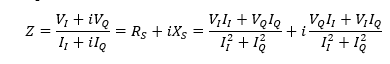
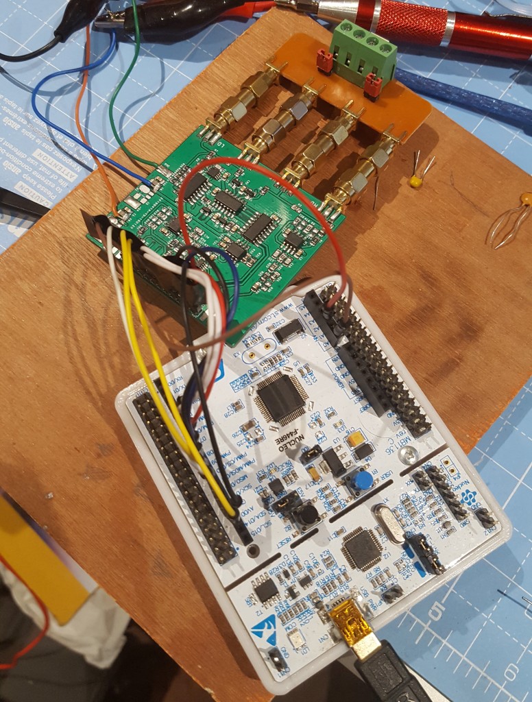
Construction:
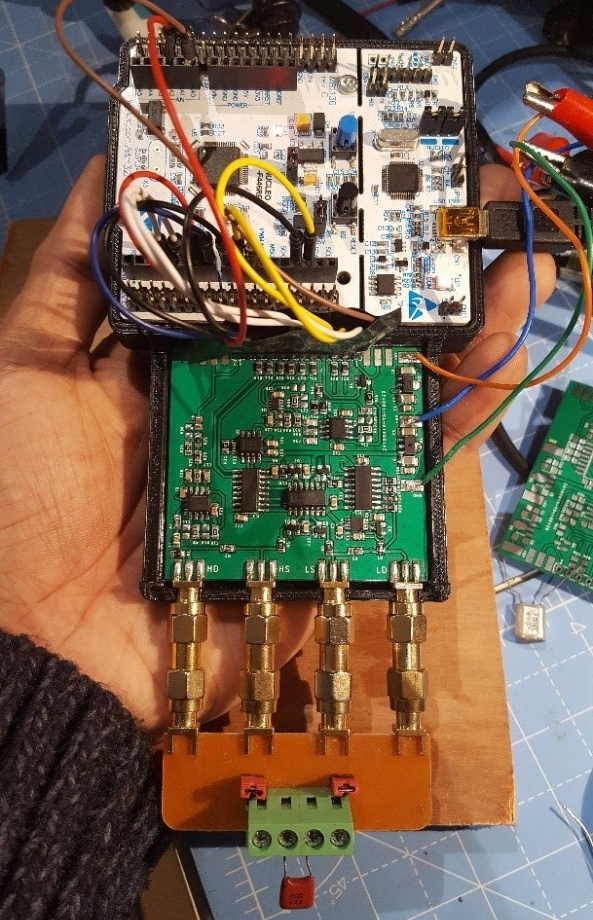
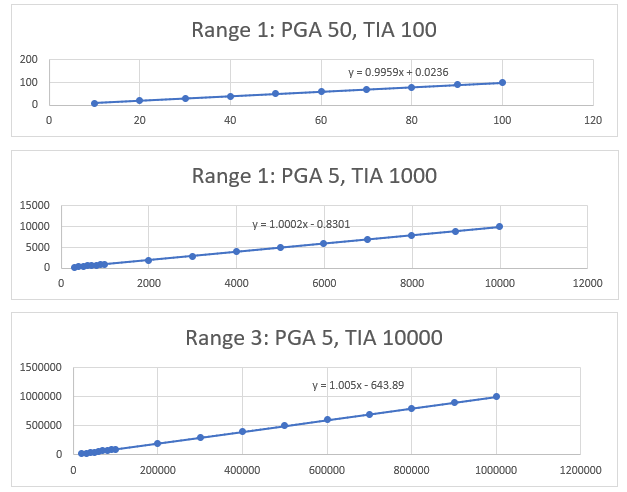
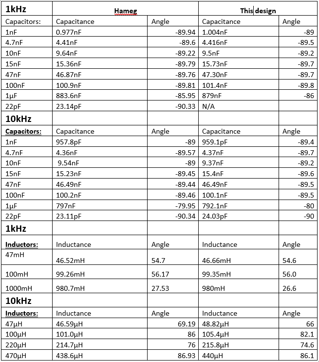
Results:
The results were surprisingly accurate for all 3 frequency ranges of 1, 10, 100 KHz.
Misc photos


Looks interesting.
Can you publish schematics and board layout ?
LikeLike
https://hackaday.com/2019/07/20/create-a-low-cost-high-accuracy-lcr-meter-with-an-stm32-mcu/
LikeLiked by 1 person
I’ve been looking for something like this for a while
any chance of sharing the schematics on github?
LikeLike
Dear Sir
Can I get Hardware and Firmware details as Project?
LikeLike